
 Q. No.
Least doped region in a transistor
(a) Either emitter or collector
(b) Base
(c) Emitter
(d) Collector
ट्रांजिस्टर में न्यूनतम अपमिश्रित क्षेत्र कौन-सा होता है?
(a) या तो उत्सर्जक या संग्राहक
(b) आधार
(c) उत्सर्जक
(d) संग्राहक


In a forward biased PN-junction diode, the potential barrier in the depletion region is of the form
1. 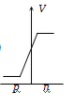
2. 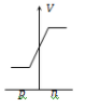
3. 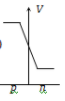
4. 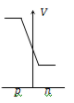
अग्र अभिनत PN संधि डायोड में, अवक्षय पर्त में विभव प्राचीर का रूप है:

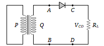
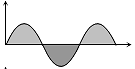
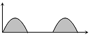
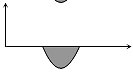
In the half-wave rectifier circuit shown. Which one of the following wave forms is true for , the output across C and D?
1. 
2. 
3. 
4. 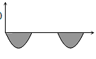
दिखाए गए अर्द्ध तरंग दिष्टकारी में, निम्नलिखित तरंग रूपों में से कौन सा C और D पर निर्गत के लिए सही है?


In a common emitter transistor, the current gain is 80. What is the change in collector current, when the change in base current is 250 A
(a) 80 250 A
(b) (250 – 80) A
(c) (250 + 80) A
(d) 250/80 A
उभयनिष्ठ उत्सर्जक ट्रांजिस्टर में, धारा लाभ 80 है। जब आधार धारा में परिवर्तन 250 A है, तब संग्राहक धारा में परिवर्तन कितना है?
(a) 80 250 A
(b) (250 – 80) A
(c) (250 +80) A
(d) 250/80 A
Which gates are represented by this figure
(1) NAND gate
(2) AND gate
(3) NOT gate
(4) OR gate
इस आरेख द्वारा कौन-से गेटों को दर्शाया जाता है?
(1) NAND गेट
(2) AND गेट
(3) NOT गेट
(4) OR गेट
The symbolic representation of four logic gates


(i) (ii)


(iii) (iv)
The logic symbols for and gates are respectively
(a) (iii), (iv), (ii) (b) (iv), (i), (iii)
(c) (iv), (ii), (i) (d) (i), (iii), (iv)
चार लॉजिक गेटों का प्रतीकात्मक निरूपण
(i) (ii)
(iii) (iv)
और गेट के लिए लॉजिक प्रतीक क्रमशः हैं
(a) (iii), (iv), (ii) (b) (iv), (i), (iii)
(c) (iv), (ii), (i) (d) (i), (iii), (iv)


In the given figure, potential difference between A and B is

(1) 0
(2) 5 volt
(3) 10 volt
(4) 15 volt
दिए गए आरेख में, A और B के मध्य विभवांतर कितना है?
(1) 0
(2) 5 volt
(3) 10 volt
(4) 15 volt
The input signal is given to a CE amplifier having a voltage gain of 150 is . The corresponding output signal will be:
1.
2.
3.
4.
CE प्रवर्धक को दिए गए निवेशी सिग्नल में 150 का वोल्टेज लाभ है। संगत निर्गत सिग्नल होगा:
1.
2.
3.
4.


An LED is constructed from a p-n junction diode using GaAsP. The energy gap is 1.9 eV. The wavelength of the light emitted will be equal to:
1. 10.4
2. 654 nm
3. 654 m
4. 654
GaAsP का उपयोग करके एक p-n संधि डायोड से एक LED का निर्माण किया जाता है। ऊर्जा का अंतर 1.9 eV है। उत्सर्जित प्रकाश की तरंग दैर्ध्य इसके बराबर होगी:
1. 10.4
2. 654 एनएम
3. 654 m
4. 654
© 2026 GoodEd Technologies Pvt. Ltd.