
 Q. No.
For the transistor circuit shown below, if = 100, voltage drop between emitter and base is 0.7 V, then value of will be :

1. 10 V
2. 5 V
3. 13 V
4. 0 V
निम्नवत दर्शाए गए ट्रांजिस्टर परिपथ के लिए, यदि = 100, उत्सर्जक और आधार के बीच विभव पतन 0.7 V है, तब का मान कितना होगा?
1. 10 V
2. 5 V
3. 13 V
4. 0 V
2. 5 V
3. 13 V
4. 0 V
2. 5 V
3. 13 V
4. 0 V


The current through an ideal p-n junction diode shown in the circuit will be -
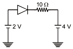
1. 5 A
2. 0.2 A
3. 0.6 A
4. Zero
परिपथ में दर्शाए गए आदर्श p-n संधि डायोड में धारा की गणना कीजिए।

1. 5 A
2. 0.2 A
3. 0.6 A
4. शून्य
In the given circuit power developed in \(1 k \Omega\) resistor is

1. 36 mW
2. 12 mW
3. 144 mW
4. 64 mW
दिए गए परिपथ में \(1 k \Omega\) प्रतिरोधक में उत्पन्न शक्ति है:
1. 36 mW
2. 12 mW
3. 144 mW
4. 64 mW


The diode shown in the circuit is a silicon diode. The potential difference between the points A and B will be
(a) 6 V

(b) 0.6 V
(c) 0.7 V
(d) 0 V
परिपथ में दर्शाया गया डायोड एक सिलिकॉन डायोड है। बिंदु A और B के मध्य विभवांतर कितना होगा?
(a) 6 V
(b) 0.6 V
(c) 0.7 V
(d) 0 V
In a common base amplifier the phase difference between the input signal voltage and the output voltage is
(a) 0 (b)
(c) (d)
उभयनिष्ठ आधार प्रवर्धक में निवेशी सिग्नल वोल्टेज और निर्गत वोल्टेज के मध्य कलांतर की गणना कीजिए:
(a) 0 (b)
(c) (d)
The transfer ratio of a transistor is 50. The input resistance of the transistor when used in the common-emitter configuration is 1 K. The peak value for an A.C input voltage of 0.01 V peak is
| 1. | 100 μ A | 2. | 0.01 mA |
| 3. | 0.25 mA | 4. | 500 μ A |
ट्रांजिस्टर का परिणमन अनुपात 50 है। उभयनिष्ठ उत्सर्जक विन्यास में उपयोग किए जाने पर ट्रांजिस्टर का निवेशी प्रतिरोध 1K है। 0.01 V के अधिकतम मान की प्रत्यावर्ती निवेशी वोल्टता के लिए प्रत्यावर्ती संग्राहक धारा का अधिकतम मान ज्ञात कीजिए।
| 1. | 100 μ A | 2. | 0.01 mA |
| 3. | 0.25 mA | 4. | 500 μ A |


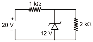
In the following circuit, find and .

(a) 0, 0
(b) 5 mA, 5 mA
(c) 5 mA, 0
(d) 0, 5 mA
निम्नलिखित परिपथ में, और ज्ञात कीजिए:
(a) 0, 0
(b) 5 mA, 5 mA
(c) 5 mA, 0
(d) 0.5 mA
The cut-in voltage for silicon diode is approximately
(a) 0.2 V (b) 0.6 V
(c) 1.1 V (d) 1.4 V
सिलिकॉन डायोड के लिए भंजक वोल्टता लगभग है:
(a) 0.2 V (b) 0.6 V
(c) 1.1 V (d) 1.4 V
The curve between charge density and distance near P-N junction will be
1. 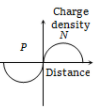
2. 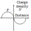
3. 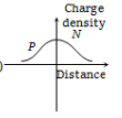
4. 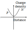
P-N संधि के निकट आवेश घनत्व और दूरी के बीच का वक्र कौन-सा होगा?
1.
2.
3.
4.


The valency of the impurity atom that is to be added to germanium crystal so as to make it an N-type semiconductor, is
(1) 6
(2) 5
(3) 4
(4) 3
अपमिश्रित परमाणु की संयोजकता ज्ञात कीजिए, जिसे जर्मेनियम क्रिस्टल में मिलाने पर इसे N-प्रकार अर्धचालक बनाया जा सकता है।
(1) 6
(2) 5
(3) 4
(4) 3
© 2026 GoodEd Technologies Pvt. Ltd.