
 Q. No.

For the logic circuit given below, the output Y for A=0, B=0 and A=1, B=1 are:
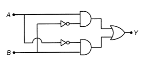
1. 0 and 1
2. 0 and 0
3. 1 and 0
4. 1 and 1


A photocell is illuminated by a point source of radiation 4 m away. If the same source is kept 8 m away, then the number of photoelectrons emitted:
1. becomes four times the initial value.
2. becomes one-fourth of the initial value.
3. remains unchanged.
4. becomes half of the initial value.


A Zener diode is used to obtain a constant voltage. If applied voltage \(\text V\) changes, then:
(\(\text V\) is more than Zener voltage)

| 1. | \(i_{1}\) and \(i_{2}\) change. |
| 2. | \(i_{2}\) and \(\text V_{0}\) change and \(i_{3}\) remains constant. |
| 3. | \(i_{2}\) and \(\text V_{0}\) don't change while \(i_{3}\) changes. |
| 4. | \(i_{3}\) and \(\text V_{0}\) don't change while \(i_{2}\) changes. |


Which of the following-junction is used unbiased?
1. Photo diode
2. LED
3. Zener diode
4. Solar cell
In the given circuit, the power developed in 2 k resistor is:
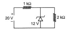
1. 36 mW
2. 12 mW
3. 144 mW
4. 72 mW
The \((I-V)\) characteristics of a \(p-n\) junction diode is as shown. If \(R_1\) and \(R_2\) be the dynamic resistance of the \(p-n\) junction when (i) a forward bias of \(1\) volt is applied and (ii) a forward bias of \(2\) volts is applied respectively, then \(\frac{R_1}{R_2}=?\)

1. \(160\)
2. \(16\)
3. \(1.6\)
4. \(0.16\)

The output of the OR gate is 1:
1. only if both inputs are zero.
2. if either or both inputs are 1.
3. only if both inputs are 1.
4. if any of the inputs is zero.
© 2024 GoodEd Technologies Pvt. Ltd.