
 Q. No.


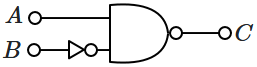


Identify the operation performed by the circuit given below:

1. \(\text{OR}\)
2. \(\text{NOT}\)
3. \(\text{NAND}\)
4. \(\text{AND}\)


The temperature dependence of resistances of \(\mathrm{Cu}\) and undoped \(\mathrm{Si}\) in the temperature range \(300\text-400~\text{K}\), is best described by:
| 1. | Linear increase for \(\mathrm{Cu}\), linear increase for \(\mathrm{Si}\) |
| 2. | Linear increase for \(\mathrm{Cu}\), exponential increase for \(\mathrm{Si}\) |
| 3. | Linear increase for \(\mathrm{Cu}\), exponential decrease for \(\mathrm{Si}\) |
| 4. | Linear decrease for \(\mathrm{Cu}\), linear decrease for \(\mathrm{Si}\) |
If \(a, b, c, d\) are inputs to a gate and \(x\) is its output, then, as per the following time graph, the gate is:

1. NOT
2. AND
3. OR
4. NAND


The Zener diode has a voltage, \(V_z=30~\text{V}.\) The current passing through the diode for the following circuit is:
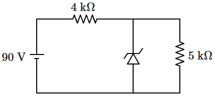
| 1. | \(3 ~\text{mA}\) | 2. | \(6 ~\text{mA}\) |
| 3. | \(9 ~\text{mA}\) | 4. | \(12 ~\text{mA}\) |
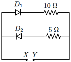
A \(5~\text{V}\) battery is connected across the points \(X\) and \(Y\). Assume \(D_1\) and \(D_2\) to be normal silicon diodes. Find the current supplied by the battery if the \(+\)ve terminal of the battery is connected to point \(X\). [Given: Barrier potential of Silicon = \(0.7~\text{V}\)]
1. \(0.5~\text{A}\)
2. \(1.5~\text{A}\)
3. \(0.86~\text{A}\)
4. \(0.43~\text{A}\)
Zener breakdown occurs in a \(\mathrm{p\text{-}n}\) junction having \(\mathrm{p}\) and \(\mathrm{n}\) both:
| 1. | lightly doped and have wide depletion layer. |
| 2. | heavily doped and have narrow depletion layer. |
| 3. | lightly doped and have narrow depletion layer. |
| 4. | heavily doped and have wide depletion layer. |


The ammeter reading for the silicon diode in the given circuit is:

1.
\(0\)
2.
\(15~\text{mA}\)
3.
\(11.5~\text{mA}\)
4.
\(13.5~\text{mA}\)
© 2025 GoodEd Technologies Pvt. Ltd.