
 Q. No.
For the given circuit of the \(\mathrm{p\text-n}\) junction diode, which of the following statements is correct?
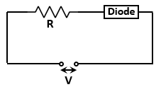
1.
In F.B. the voltage across \(R\) is \(V\).
2.
In R.B. the voltage across \(R\) is \(V\).
3.
In F.B. the voltage across \(R\) is \(2V\).
4.
In R.B. the voltage across \(R\) is \(2V\).


The following truth table represent which logic gate:
| A | B | C |
| 1 | 1 | 0 |
| 0 | 1 | 1 |
| 1 | 0 | 1 |
| 0 | 0 | 1 |
1. XOR
2. NOT
3. NAND
4. AND
The current \((I)\) in the circuit will be:

| 1. | \(\dfrac{5}{40}~\text{A}\) | 2. | \(\dfrac{5}{50}~\text{A}\) |
| 3. | \(\dfrac{5}{10}~\text{A} \) | 4. | \(\dfrac{5}{20}~\text{A}\) |


Reverse-bias applied to a junction diode:
| 1. | lowers the potential barrier |
| 2. | raises the potential barrier |
| 3. | increases the majority carrier current |
| 4. | increases the minority carrier's current |
If a full-wave rectifier circuit is operating from \(50~\text{Hz}\) mains, the fundamental frequency in the ripple will be:
1. \(25~\text{Hz}\)
2. \(50~\text{Hz}\)
3. \(70.7~\text{Hz}\)
4. \(100~\text{Hz}\)
The barrier potential of a \(\mathrm{p\text-n}\) junction diode does not depend on:
1. diode design
2. temperature
3. forward bias
4. doping density
Following diagram performs the logic function of:

1. AND gate
2. NAND gate
3. OR gate
4. XOR gate
| A | B | Y |
| \(1\) | \(1\) | \(0\) |
| \(0\) | \(1\) | \(1\) |
| \(1\) | \(0\) | \(1\) |
| \(0\) | \(0\) | \(1\) |
2. XOR
3. NOR
4. OR
| 1. | High potential at the \(\mathrm{n}\) side and low potential at the \(\mathrm{p}\) side. |
| 2. | High potential at the \(\mathrm{p}\) side and low potential at the \(\mathrm{n}\) side. |
| 3. | \(\mathrm{p}\) and \(\mathrm{n}\) both are at the same potential. |
| 4. | Undetermined. |
The output of the OR gate is \(1\):
| 1. | if either or both inputs are \(1.\) |
| 2. | only if both inputs are \(1.\) |
| 3. | if either input is zero |
| 4. | if both inputs are zero |
© 2024 GoodEd Technologies Pvt. Ltd.