- 1(current)
 Q. No.
| 1. | in the case of \(C\), the valence band is not completely filled at absolute zero temperature. |
| 2. | in the case of \(C\), the conduction band is partly filled even at absolute zero temperature. |
| 3. | the four bonding electrons in the case of \(C\) lie in the second orbit, whereas in the case of \(Si\), they lie in the third. |
| 4. | the four bonding electrons in the case of \(C\) lie in the third orbit, whereas for \(Si\), they lie in the fourth orbit. |
Prefer Books for Question Practice? Get NEETprep's Unique MCQ Books with Online Audio/Video/Text Solutions via Telegram Bot
NEET MCQ Books for XIth & XIIth Physics, Chemistry & Biology1. \(6000~\mathring{A}\)
2. \(4000\) nm
3. \(6000\) nm
4. \(4000~\mathring{A}\)
Prefer Books for Question Practice? Get NEETprep's Unique MCQ Books with Online Audio/Video/Text Solutions via Telegram Bot
NEET MCQ Books for XIth & XIIth Physics, Chemistry & BiologyA p-n photodiode is made of a material with a bandgap of 2.0 eV. The minimum frequency of the radiation that can be absorbed by the material is nearly:
1.
2.
3.
4.
Prefer Books for Question Practice? Get NEETprep's Unique MCQ Books with Online Audio/Video/Text Solutions via Telegram Bot
NEET MCQ Books for XIth & XIIth Physics, Chemistry & BiologyIn the energy band diagram of a material shown below, the open circles and filled circles denote holes and electrons respectively. The material is a/an:
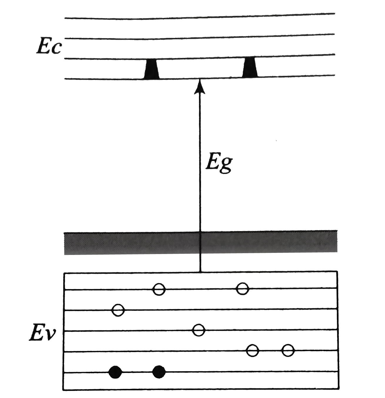
1. p-type semiconductor
2. insulator
3. metal
4. n-type semiconductor
Prefer Books for Question Practice? Get NEETprep's Unique MCQ Books with Online Audio/Video/Text Solutions via Telegram Bot
NEET MCQ Books for XIth & XIIth Physics, Chemistry & Biology- 1(current)
Q. No.© 2024 GoodEd Technologies Pvt. Ltd.