In the circuit shown in the figure, the input voltage Vi is 20 V, VBE = 0, and VCE = 0. The values of IB, IC and are given by:
1.
2.
3.
4.
The given electrical network is equivalent to:
| 1. | \(\text{OR}\) gate | 2. | \(\text{NOR}\) gate |
| 3. | \(\text{NOT}\) gate | 4. | \(\text{AND}\) gate |
If in a \(\mathrm{p\text{-}n}\) junction, a square input signal of \(10~\text{V}\) is applied as shown,
then the output across \(R_L\) will be:
| 1. |  |
2. |  |
| 3. |  |
4. |  |
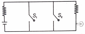
Two ideal diodes are connected to a battery as shown in the circuit. The current supplied by the battery is:
| 1. | \(0.75~\text{A}\) | 2. | zero |
| 3. | \(0.25~\text{A}\) | 4. | \(0.5~\text{A}\) |
Transfer characteristics [output voltage () vs input voltage ()] for a base biased transistor in CE configurations are as shown in the figure. For using the transistor as a switch, it is used:
1. In region III
2. Both in the region (I) and (III)
3. In region II
4. In region I
In the following circuit, the output \(Y\) for all possible inputs \(A\) and \(B\) is expressed by the truth table:

| 1. | A | B | Y | 2. | A | B | Y |
| 0 | 0 | 0 | 0 | 0 | 1 | ||
| 0 | 1 | 0 | 0 | 1 | 1 | ||
| 1 | 0 | 0 | 1 | 0 | 1 | ||
| 1 | 1 | 1 | 1 | 1 | 0 | ||
| 3. | 0 | 0 | 1 | 4. | 0 | 0 | 0 |
| 0 | 1 | 0 | 0 | 1 | 1 | ||
| 1 | 0 | 0 | 1 | 0 | 1 | ||
| 1 | 1 | 1 | 1 | 1 | 1 |
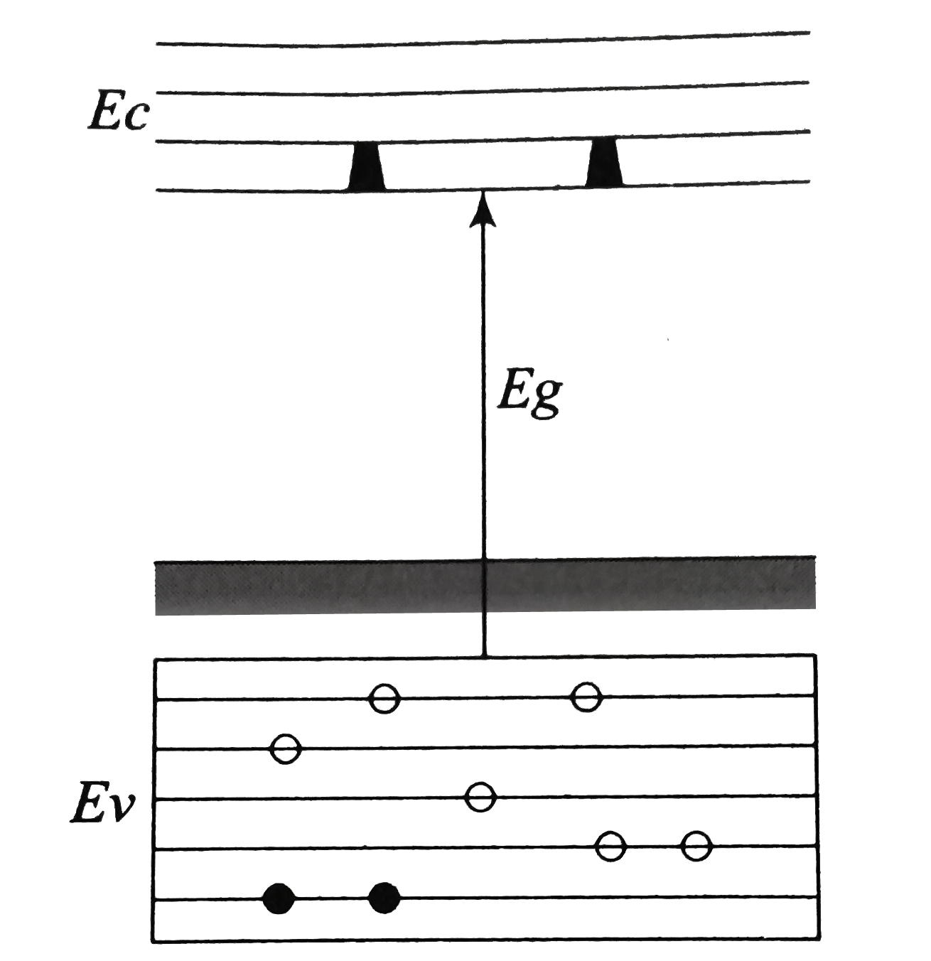
In the energy band diagram of a material shown below, the open circles and filled circles denote holes and electrons respectively. The material is a/an: 
1. p-type semiconductor
2. insulator
3. metal
4. n-type semiconductor
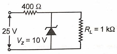
A Zener diode of breakdown voltage, = 10 V is used in the given circuit. The current through the load resistor is:

1. 10
2. 5
3. 10 mA
4. 5 mA
Choose the incorrect statement for the full-wave rectifier out of the following statements:
1. Maximum theoretical efficiency is 81.2%
2. A DC-ammeter connected to the output of rectifier reads current where is the peak value of current In the circuit
3. An AC-ammeter connected to the output of rectifier reads current where is the peak value of current in the circuit
4. The ripple factor is greater than one.
The circuit shown below is equivalent to:

1. OR gate
2. NOR gate
3. AND gate
4. NAND gate
In an n-p-n transistor circuit, the collector current is 10 mA. If 95 percent of the electrons emitted reach the collector, which of the following statements are true?
1. The emitter current will be 8 mA
2. The emitter current will be 10.53 mA
3. The base current will be 5.53 mA
4. The base current will be 2mA
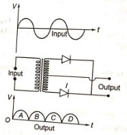
A full-wave rectifier circuit along with the input and output are shown in the figure, the contribution from the diode I is (are):
1. C
2. A, C
3. B, D
4. A, B, C, D
Doping of a semiconductor (with small traces of impurity atoms) generally changes the resistivity as follows:
1. does not alter
2. increases
3. decreases
4. may increase or decrease depending on the dopant